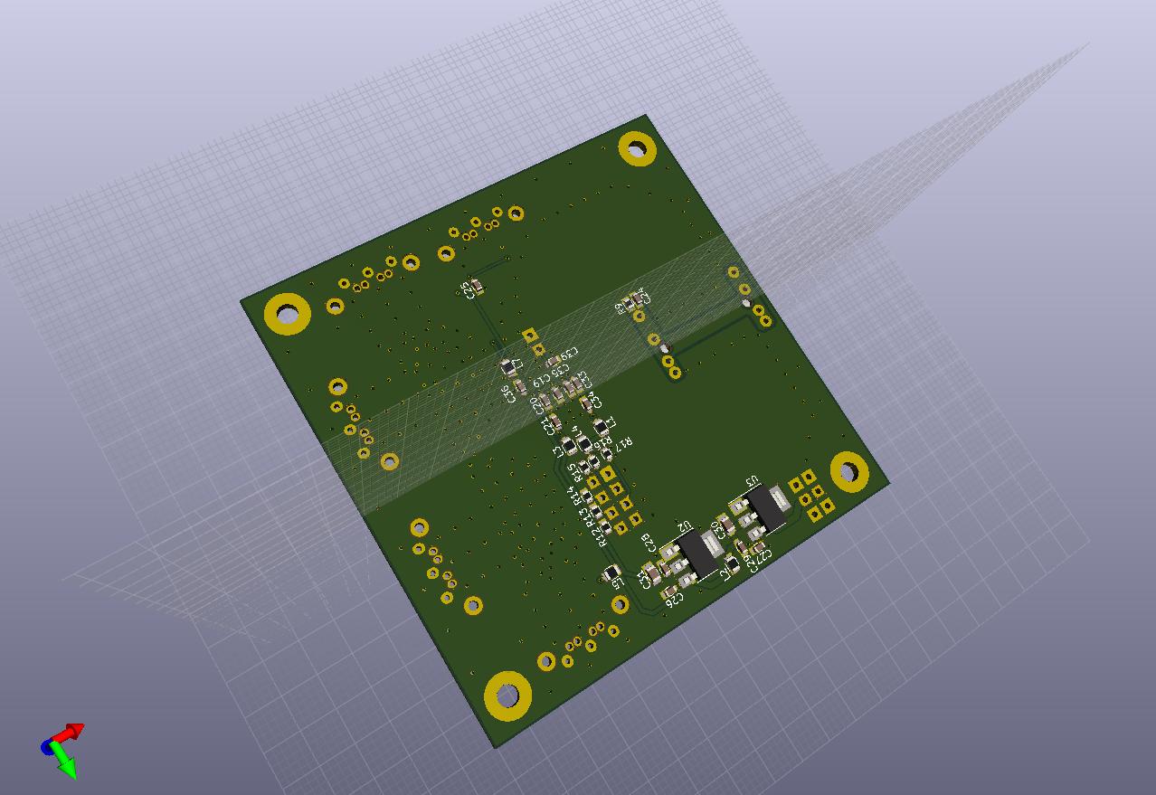
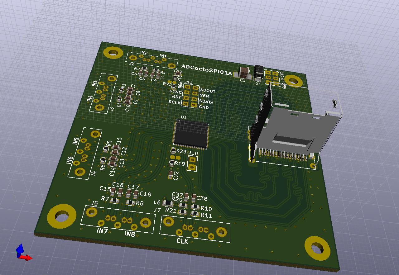
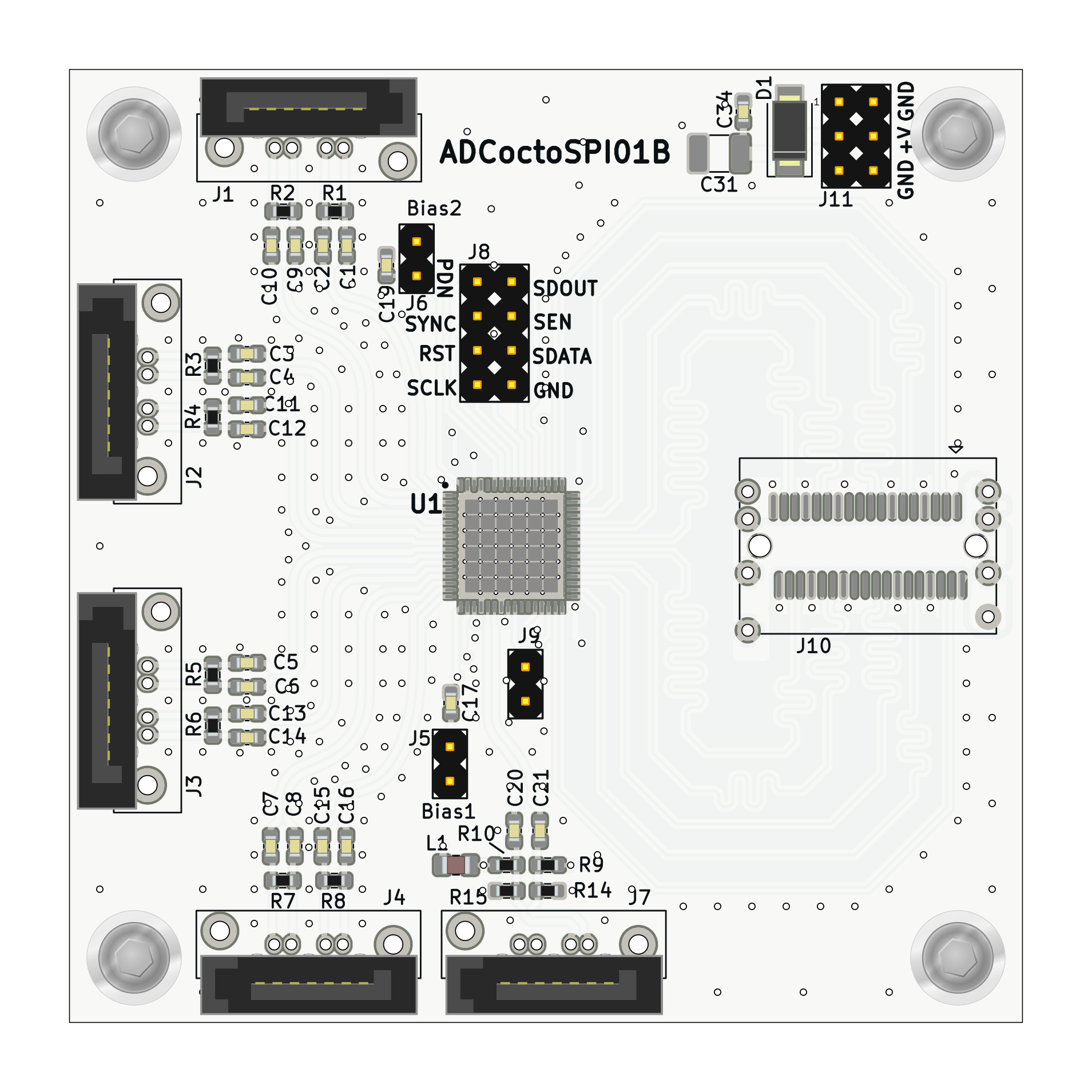
ADCoctoSPI01 - Octal Input High-Speed ADC Module
The ADCoctoSPI01 is an eight-channel, high-speed analog-to-digital conversion module designed for signal acquisition in imaging and similar high-speed applications. It integrates a Texas Instruments AFE5801 analog front-end (AFE), which combines eight variable-gain amplifiers (VGAs) and eight 12-bit ADCs with a sampling rate up to 65 MSPS. Data output is serialized through an LVDS interface.

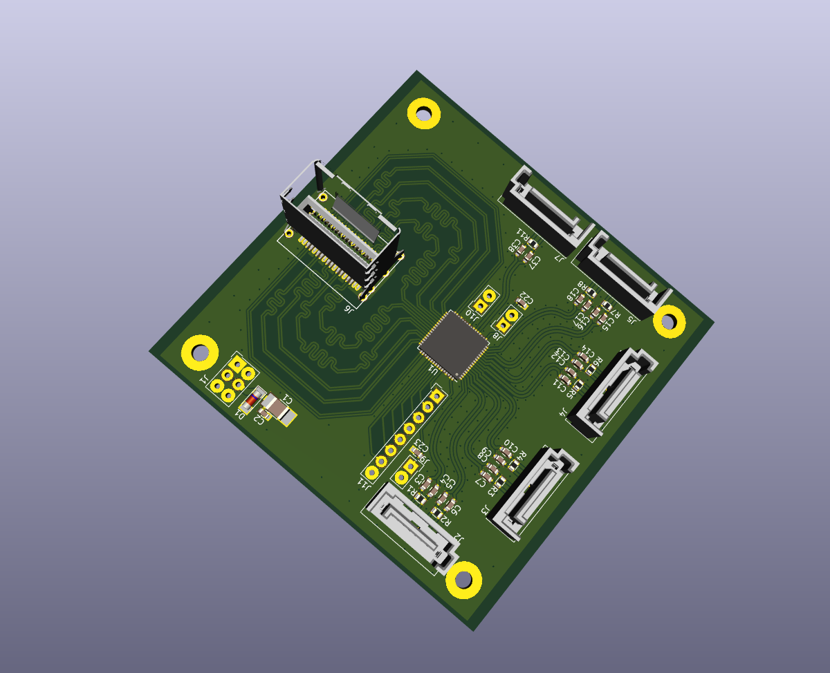
This module is ideally used in combination with the MPPB01 baseboard for Parallella, which features a compatible miniSAS connector, allowing for direct integration and high-speed data transfer.
Features
- 8 differential analog input channels
- Integrated AFE5801 from Texas Instruments
- 8x VGAs with -5 dB to 31 dB gain range
- 8x 12-bit ADCs, up to 65 MSPS sampling rate
- Integrated anti-aliasing filter (7.5 / 10 / 14 MHz selectable)
- Serial LVDS output
- SPI control interface
- MiniSAS (SFF-8087) connector for LVDS data output
- Separate SPI interface for configuration and diagnostics
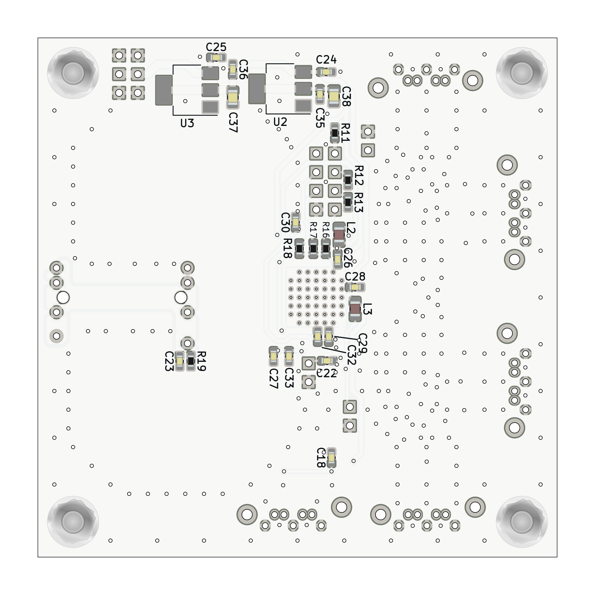
- On-board linear regulators for 1.8V and 3.3V supplies
- Operating voltage: 3.6 V to 5.4 V
- Operating temperature: -20 °C to +40 °C
Technical Specifications
| Parameter |
Value |
Description |
| ADC Resolution |
12 bits |
Per channel |
| Number of Channels |
8 |
Differential |
| Max Sampling Rate |
65 MSPS |
Per channel |
| Input Voltage Swing |
2 Vpp |
Differential, max linear input range |
| VGA Gain Range |
-5 dB to +31 dB |
Step size: 0.125/1 dB |
| Input Referred Noise |
5.5 nV/√Hz |
At VGA gain = 31 dB |
| Signal-to-Noise Ratio (SNR) |
~65 dBFS |
Typical at 65 MSPS, -1 dBFS input |
| Total Harmonic Distortion (THD) |
-65 dBFS |
At 5 MHz input, max gain |
| Signal-to-Noise and Distortion Ratio (SINAD) |
~68 dB |
|
| Antialias Filter Cutoff |
7.5 / 10 / 14 MHz |
Programmable |
| Common-Mode Input Voltage (VCM) |
1.6 V |
Recommended bias for AC coupling |
| Input Capacitance |
2 pF |
Differential input |
| Input Resistance |
5 kΩ |
To internal bias |
Connectors
- J1-J4: Differential analog inputs (IN1P/M to IN8P/M) (SATA connectors)
- J10A: MiniSAS connector for serialized LVDS data (D1-D8, FCLK, DCLK)
- J8: SPI control interface (SCLK, SDATA, SDOUT, SEN, RESET, SYNC)
- J11: Power input (+5V, GND)
Power Supply
- Requires a single 5V power supply.
- Onboard regulators generate 3.3V and 1.8V for AFE operation.
AFE5801 Configuration Highlights
- Gain Control: SPI-controlled VGA gain, from -5 dB to 31 dB in 0.125 dB or 1 dB steps
- Clamping and Filtering: Optional signal clamping and integrated third-order low-pass filter
- Sampling Clock: Differential clock input (LVDS/PECL supported)
- LVDS Output: Serialized outputs for each channel (D1-D8), frame clock (FCLK), and data clock (DCLK)
Typical Applications
- Medical ultrasound systems
- Non-destructive testing
- High-speed data acquisition
- Multichannel signal digitization in SDR receivers
References
- AFE5801 Datasheet
- Other compatible AFEs: AFE5805, AFE5809 (with differing performance and power specs)
Notes
- Only the AFE5801 is populated by default; board supports footprint-compatible variants (AFE5803, AFE5804 etc.).
- For optimal performance, ensure proper analog signal termination and impedance matching on all differential inputs.
- Follow ESD precautions during handling.