


ADSBAFE01 is a complete 1090 MHz analog front-end for ADS-B / Mode-S reception. The module integrates RF filtering, low-noise amplification, logarithmic power detection and high-speed pulse shaping. It is intended to deliver a logic pulse stream corresponding to the RF envelope together with auxiliary RSSI information for sensitivity control and signal quality evaluation.
ADSBAFE01 is designed as an analog front-end for custom ADS-B receivers where digital demodulation and message decoding are implemented externally (MCU, FPGA, SDR backend, etc.). The module does not perform protocol decoding; it delivers time-accurate envelope pulses and auxiliary RSSI information for higher-layer processing.
The RF signal enters through a 50 Ω MCX connector and immediately passes a 1090 MHz SAW band-pass filter (~30 MHz bandwidth). This suppresses strong out-of-band signals before amplification. The filtered signal is amplified by a BGA2818 LNA with approximately +30 dB gain. Then logarithmic power detector (AD8313) converts the RF envelope into a baseband voltage proportional to signal level. This node is intentionally kept lightly loaded because additional capacitance directly degrades slew rate and therefore timing accuracy of the detected pulses (see schematic notes ).
The detector output is processed in two parallel paths:
This separation allows reliable time-domain decoding while still exposing signal strength information for adaptive thresholding or diagnostics.
The comparator (MCP6566) converts the detector voltage into a CMOS pulse stream. Its propagation delay is on the order of 50 ns with ~20 ns fall time, which is sufficient for 1 µs ADS-B pulses.
The detection threshold is not fixed. It is derived from bias networks controlled by a 100 kΩ digital potentiometer (MCP4017, I²C). This allows software-controlled sensitivity adjustment without hardware modification. Low-frequency RC filtering in the bias network (fc ≈ 159 Hz) stabilizes the reference and suppresses slow variations.
The resulting PULSES output can be directly connected to:
For signal strength evaluation, the module implements an active peak detector (op-amp based). During a decode window, the peak value of the (inverted) log-detector output is sampled and held. The reset discharge time constant is approximately 44 ns, with ~95 % discharge in ~132 ns, enabling packet-level RSSI measurements without excessive memory between adjacent pulses.
The analog RSSI signal can be read by an external ADC if quantitative signal strength estimation is required.
| Parameter | Value / Description |
|---|---|
| Supply voltage | 3.3 V |
| RF frequency | 1090 MHz (ADS-B / Mode-S) |
| RF input impedance | 50 Ω |
| LNA gain | ~+30 dB |
| Comparator delay | ~50 ns |
| Logic levels | 3.3 V CMOS |
| Threshold control | I²C digital potentiometer |
The module includes input decoupling (10 µF + 100 nF) and supply protection (TVS diode) as shown in the schematic .
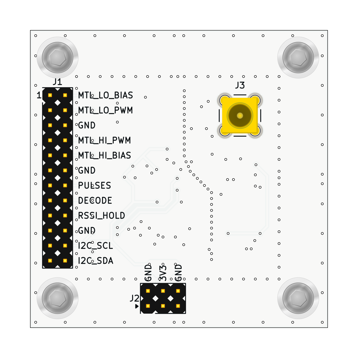
Type: MCX with impedance: 50 Ω
The IO header exposes digital control, RSSI and interface signals. Series resistors provide basic IO protection and edge damping.
| Signal | Direction | Description |
|---|---|---|
| PULSES | Output | Digital ADS-B envelope pulses |
| RF_LEVEL | Output (analog) | Log-detector RSSI voltage |
| DECODE | Input | Enables RSSI peak sampling |
| RSSI_HOLD | Input | Controls sample/hold state |
| RSSI_DSCHRG | Input | Forces RSSI capacitor discharge |
| MTL_HI_PWM | Input | Comparator reference control (high) |
| MTL_LO_PWM | Input | Comparator reference control (low) |
| MTL_HI_BIAS | Internal / test | Bias node (high threshold) |
| MTL_LO_BIAS | Internal / test | Bias node (low threshold) |
| I2C1_SCL | Input | I²C clock (digital potentiometer) |
| I2C1_SDA | Bidirectional | I²C data |
| +3V3 | — | Supply |
| GND | — | Ground |