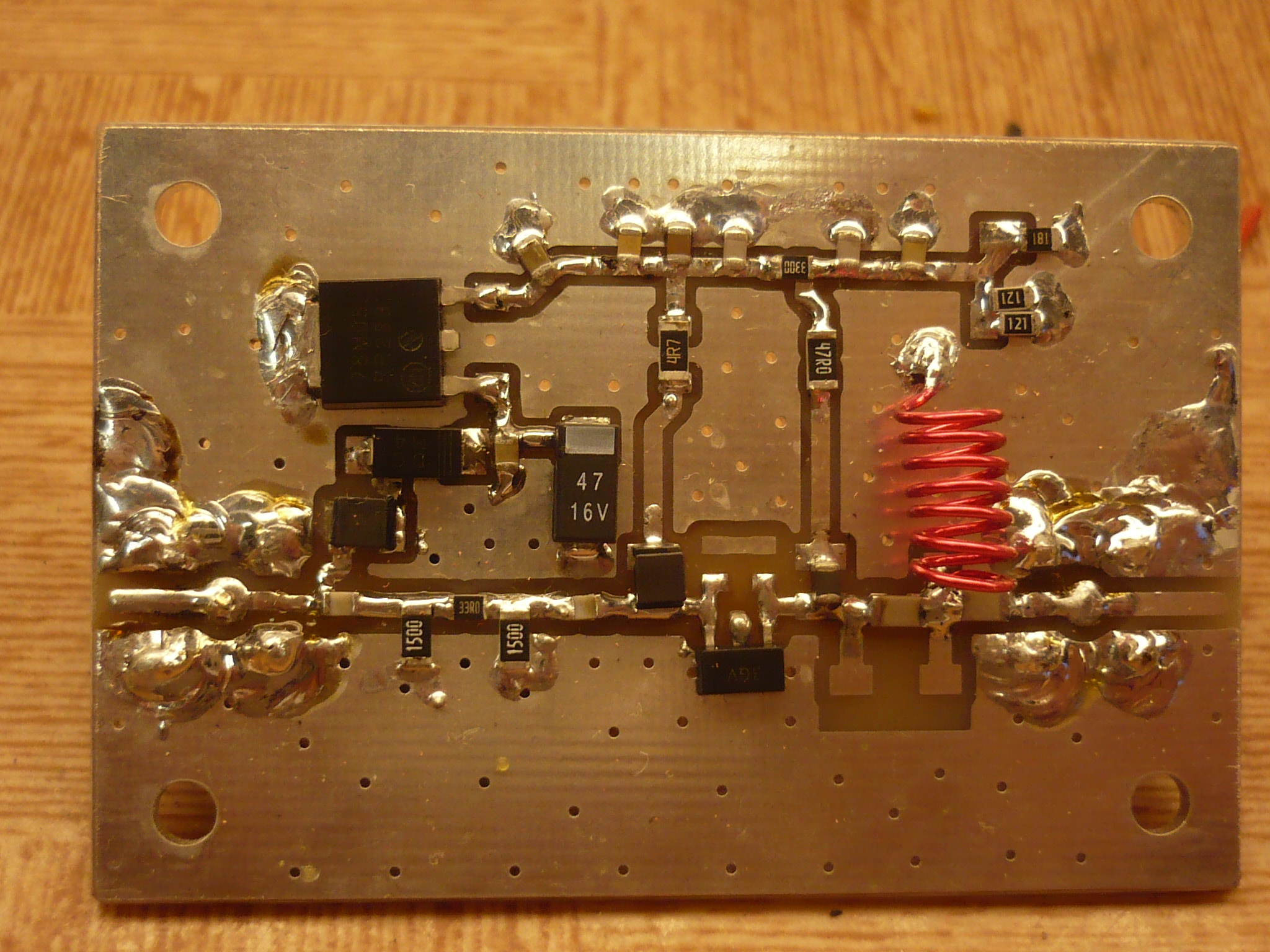
Author: Jakub Kákona, kaklik@mlab.cz
Abstract
An input low noise amplifier designed for band amplification of signals immediately after the antenna. It is optimized for very low noise to enable the construction of receiver setups with a low noise figure.
| Parameter | Value | Note |
|---|---|---|
| Power Supply Voltage | up to +12V | max 200mA |
| Frequency Range | 100 - 200 MHz | With different components, up to 450MHz |
| Maximum RF Input Power | + 24 dBm | Maximum 1V at RF input |
| OIP3 | 40dBm | |
| Noise Figure | < 0.8 dB |
The amplifier's circuit is implemented on an FR4 printed circuit board (PCB). The PCB can be equipped with either direct SMA connectors or edge connectors.
The amplifier must necessarily be housed in a metal shielding box to prevent it from being excited by signals emitted to the antenna. The metal box also ensures higher signal quality from the amplifier output.
It is assumed that the amplifier will be placed in a tin-plated metal shielding box in which the amplifier is soldered behind the connectors. Holes for connectors are created in the box using punching pliers with a diameter tool of 6.35mm. A template named hole_pattern.pdf is used for punching these holes.
The assembly of SMD components is carried out using solder paste, including the transistor. Special attention must be paid to antistatic protection during the transistor assembly to prevent damage. The transistor can only be soldered using electrostatically safe tools, such as hot air or IR solder.
After soldering the SMD components, an air coil can be soldered, which may be soldered using a contact solder. It is advisable to use a higher power solder to securely solder the coil to the ground plane.
Finally, after fully soldering the coil, the amplifier's input and output can be short-circuited, which are short-circuited by the non-etched copper layer on the opposite side of the SMD components at the PCB factory. Therefore, it is necessary to clear the hole for the SMA connector center, which can best be done with a drill of about 8mm in diameter.